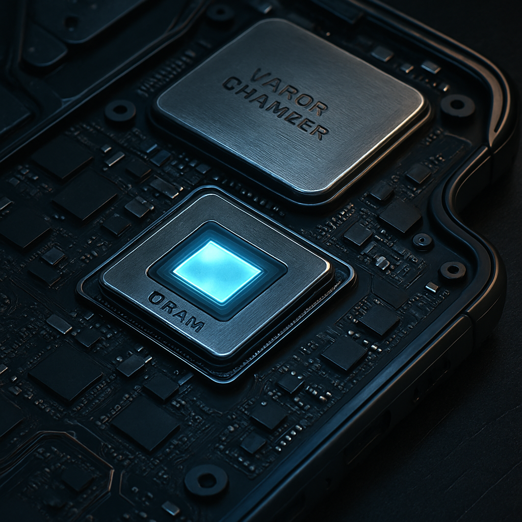
Apple’s latest chip, the A20 Pro, made its debut inside the iPhone 18 Pro, Pro Max, and iPhone Duo. It’s the company’s first chip built using a 2-nanometer process, delivering about 20% faster CPU performance and a 40% boost on the GPU front. But raw node shrinks are just part of the story
What makes A20 Pro special
Apple’s silicon division emphasizes that designing a chip isn’t just about adopting the latest manufacturing process. Architecture, layout, package design, system integration and how software, cooling, and memory all work together matter just as much. The A20 Pro benefits from a host of coordinated upgrades: more neural engine capacity, extra GPU cores, expanded memory channels, and a revised packaging layout that changes where DRAM sits relative to the chip package.
A key element is thermal management. By placing the chip directly above the phone’s vapor chamber cooling system and shifting DRAM from the top to the side edge, Apple managed to improve heat dissipation, enabling stronger sustained performance. That layout comes at the cost of a slightly larger footprint, but cooperation between different engineering teams ensured the logic board accommodates the change.
Built for future use cases
Another striking point: Apple didn’t stop at delivering gains for today. During A20 Pro’s design, teams factored in what future features might demand. Decisions like selecting sufficient memory bandwidth or integrating headroom for camera innovations or AI functions had to be made years in advance—even if the use case isn’t live yet.
Apple isn’t building these chips for anyone else. Because its silicon, hardware, and software are developed in sync, the company avoids the compromises typical in “merchant silicon”—chips designed for many customers rather than tailored to a single product line. This vertical integration shows through not just in peak performance, but in how the parts around the chip—cooling, DRAM, package, firmware—are optimized to meet Apple’s specific product expectations.
The use of a leading-edge 2nm process gave Apple more transistor density. That bounty enabled extra GPU cores, higher neural engine capacity, and broader memory channels—features that contribute to both raw performance and the ability to handle more ambitious AI workloads without overheating or throttling too quickly.
All told, A20 Pro is not just a generation-over-generation bump. It’s a rethinking of how a modern smartphone SoC is built—where performance, cooling, packaging and future readiness all get designed together rather than as separate parts.
What this means: A20 Pro represents Apple’s strategy of owning the full stack—from silicon to system—to achieve not just faster benchmarks but more stable, long-term performance. For users, this means devices that feel faster and cooler, especially under demanding tasks like AI or video processing. From a tech-industry perspective, Apple continues to push the benchmark for what vertically integrated product engineering can achieve. The biggest watch-points now are whether competitors can match not just chip node shrinks, but the holistic system design that gives these alone room to shine.