Apple’s M6 chip, unveiled with the new Mac mini in August, marks the company’s first foray into 2-nanometer process technology for desktop silicon. This shift from the M5’s N3P node to a smaller N2 node enables tighter component packing and substantial performance enhancements. Early die-shot analyses from High Yield and SemiAnalysis confirm the physical differences and structural changes that underpin these gains.
From N3P to N2: Die Shrink and Die Size
The M5 die occupies roughly 154 square millimeters, measuring 12.75mm by 12.08mm. The M6, even with its upgraded architecture, manages to shrink in size to about 141.6 square millimeters—12.8mm by 11.06mm—thanks to the move to N2 technology. While smaller, the M6 still maintains comparable or enhanced capabilities in many key areas.
Core Layout, Cache, and Performance Configurations
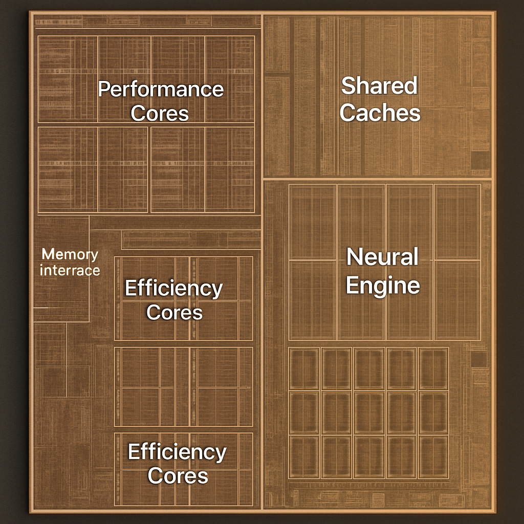
The CPU core arrangement has been overhauled: Apple scaled back from four super cores plus six efficiency cores in the M5 to two super cores, four performance cores, and six efficiency cores in the M6. In the die images, the two super cores appear large yet more compact than in the M5, with each now equipped with a larger 1.5-megabyte private L2 cache.
Shared caches also got an upgrade: the unified shared L2 cache for the S- and P-cores now totals 10MB—4MB more than in the M5. The efficiency core cluster includes six cores sharing 8MB of cache, up from the M5’s 6 cores sharing 6MB. Apple also added an AMX unit to the E-core cluster to aid matrix math computations.
Memory, GPU, and Neural Engine Tweaks
Memory bandwidth varies by configuration. The 16GB M6 maintains the same DRAM spec as the M5—9,600 MT/s—yielding equal bandwidth. Larger M6 models (24GB and 32GB) step up to 10,667 MT/s DRAM, boosting bandwidth to about 170GB/s. On the GPU side, two extra cores come with about a 10% shrink in per-core size due to the denser process.
The Neural Engine doubles its core count compared to prior chips and gains a more balanced layout. It’s organized as two clusters of eight dual-core blocks, each with cache, hooked into a central controller. Peripheral I/O remains largely similar, though the M6 shows upgrades in PCI-Express lane configuration—possibly six lanes of Gen 4—versus the M5’s mix of Gen 4 and Gen 3 lanes. PHYs for display and camera continue to use dedicated lanes.
What’s Next: Looking Toward M7
The M6 appears likely to be a shorter generation, with expectations pointing toward an AI-focused M7 arriving within months. One major change might involve the memory interface: the M-series has used a 128-bit interface since the M1, while Apple’s recent A20 chips adopt a wide 96-bit interface. The mobile-inspired basis of the M chips suggests that a similar interface shift could be on the way with M7.
Why this matters: Apple’s adoption of the 2nm N2 process with the M6 shows continuing leadership in chip efficiency and performance scaling. By squeezing more function into less silicon, Apple can deliver higher throughput, better power behavior, or both. The changes in core configuration, cache sizes, and memory bandwidth won’t be dramatic on paper alone—but together they point to meaningful gains in day-to-day performance. Keep an eye on how the AI demands of upcoming workloads press Apple’s design team, particularly around the memory interface and bandwidth, since that may define the edge in future generations.