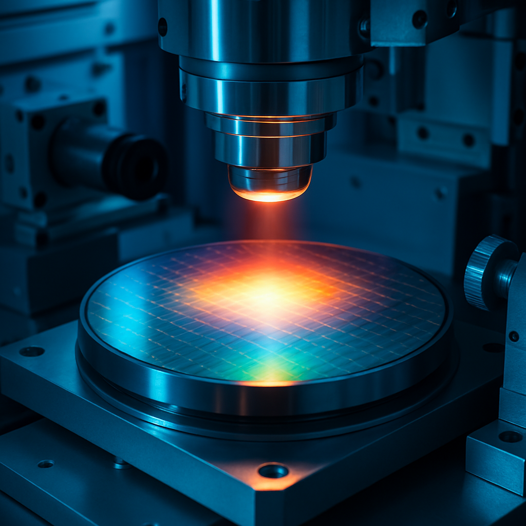
In the face of growing limitations in traditional silicon-based transistors—issues like leakage, overheating, and inefficiencies—Singapore startup Nexstrom is betting the future lies in atomically-thin materials. The company is developing processes and equipment that would allow foundries to integrate transition-metal dichalcogenides (TMDs)—a class of ultra-thin materials usually just a few atomic layers thick—directly onto commercial chipmaking wafers. These “2D” materials offer a path forward as the shrinking of silicon-based transistors becomes ever more challenging.
Nexstrom says its flagship product, called North Star, is built to grow TMDs on standard 300 mm (12-inch) wafers, the size already widely used in semiconductor fabs. Foundries currently working with 200 mm or 300 mm substrates would be the immediate target users. Equipment-makers and lab researchers worldwide have long studied 2D semiconductors, but the challenge has been scaling up: creating high-quality, uniform materials at wafer scale. Nexstrom claims to have made significant progress here.
Scaling Up: From Lab to Fab
The company has already installed a 12-inch system and has demonstrated material quality at that level. It reports having scaled up production across multiple wafer sizes: from 2-inch to 6-inch so far. Nexstrom expects to complete trials on 8-inch wafers by the end of October. Forming reliable TMD layers across whole wafers—and meeting the stringent material specifications demanded by commercial fabs—is its current major hurdle.
Nexstrom was co-founded by Lance Li, formerly a lead researcher in post-silicon electronics at one of the world’s biggest contract chipmakers. Li has studied 2D materials research since around 2012 and brings both scientific deep knowledge and industry credibility. The startup is positioning itself not to compete head-on with giants such as TSMC, Intel, or Samsung, but rather to partner or sell its technology to them. It says that some potential customers are already testing samples of its wafers or materials.
Funding, Timeline, and Commercialization
This week Nexstrom closed a $12 million seed round, bringing its total funding to $15 million. Key backers include Xora Innovation, Foothill Ventures, and SEEDS. The investment will support improvements in process control, measurement systems, team expansion, and qualification programs with chip manufacturers.
While Nexstrom’s systems are showing promise, commercial production readiness is still ahead. The company projects that its equipment could be certified and in use for production between 2030 and 2035. That timeline reflects the scale of the scientific, engineering, and manufacturing validation needed so fabs can trust these new materials.
Globally, other players—such as IMEC, TSMC, Intel—and equipment suppliers like AIXTRON and emerging startups are exploring different approaches to embed 2D materials into transistor design. Some recent demonstrations have shown integration of 2D semiconductors in 300 mm processes, but maintaining quality and consistency at that size remains difficult.
Swiftly moving from lab-scale success to fab-scale confidence is the crux. Nexstrom’s work to meet industry specs across large wafers—and its collaborations already underway—might make 2D semiconductors a mainstream route past silicon’s scaling limits. If those efforts succeed, the story of Moore’s Law’s next chapter may soon include Singapore’s name as a major contributor.